Arsenic: The Toxic Critical Mineral Powering GaAs Semiconductors for AI
- David Rogers
- AI Buildout Supply Chain
- 2026-07-06
NEED TO KNOW
- Essential for High-Speed GaAs: High-purity (6N+) arsenic is synthesized with gallium into GaAs compound semiconductors for VCSEL arrays, high-frequency RF, and photonic interconnects.
- Severe Supply Concentration: The US has no active domestic primary arsenic production, relying on China for ~95–96% of metallic arsenic imports alongside Peru and Morocco.
- Toxicity & Environmental Control: Extreme toxicity and strict hazardous waste regulations inflate manufacturing costs versus silicon, requiring rigorous fab containment systems.
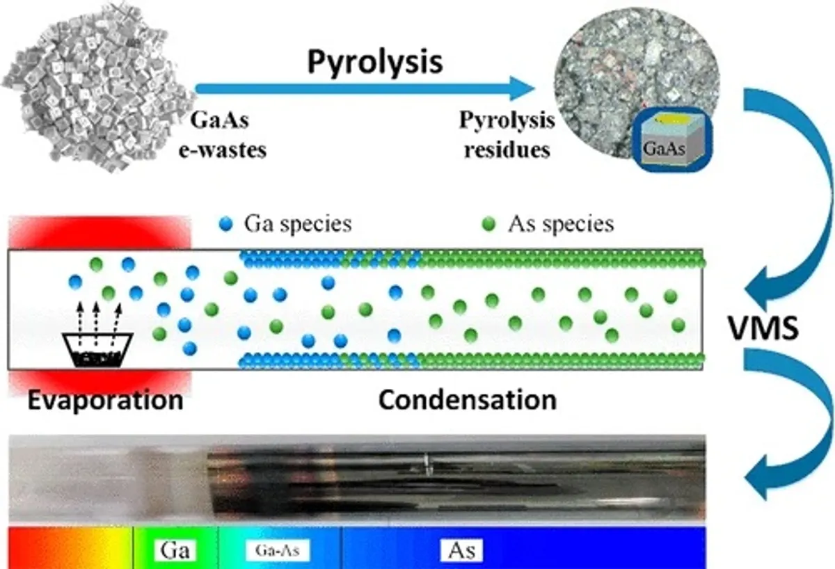
- Scrap Recycling Opportunities: Advances in vacuum-thermal decomposition and hydrochemical scrap processing achieve 85–95% recovery of high-purity Ga and As from GaAs manufacturing waste.
Arsenic is the critical and highly problematic feedstock that makes gallium arsenide (GaAs) compound semiconductors possible. GaAs excel where silicon hits physical limits: superior electron mobility and direct bandgap enable high-frequency RF/power amplifiers (critical for 5G/6G base stations and wireless edge AI), optoelectronic devices (Vertical-Cavity Surface-Emitting Laser or VCSEL), and specialized photonics or defense-grade chips. In AI infrastructure, GaAs VCSEL arrays support energy-efficient optical interconnects in data centers /Chalmers/ that reduce power and latency for massive AI training/inference clusters while RF components enable low-latency wireless backhaul and distributed intelligence.
Producing electronic-grade GaAs demands extreme purity and specialized handling /LibreText/. Arsenic arrives primarily as a toxic byproduct of copper, gold, and lead smelting; it is refined to 6N (99.9999%) or higher purity metal. High-purity gallium (also 6N–7N, often from bauxite) reacts with arsenic vapor in sealed ampoules to synthesize polycrystalline GaAs. Single-crystal ingots then grow via liquid encapsulated czochralski (LEC), using boron trioxide to contain volatile arsenic, or vertical gradient freeze (VGF) for lower defect densities. Ingots are sliced into wafers (mostly 6-inch, some 8-inch), polished, and receive epitaxial layers via metalorganic chemical vapour deposition (MOCVD) or molecular-beam epitaxy (MBE) for device structures. Trace impurities at parts-per-million (ppm) or sub-ppm levels destroy carrier mobility, introduce recombination centers, or degrade optical performance, so zone refining and Bridgman purification are essential.
Key challenges center on cost, toxicity, and yield. Arsenic’s extreme toxicity requires specialized containment, waste treatment, and regulatory compliance /EPA/, inflating expenses versus silicon. LEC growth produces higher dislocation densities; scaling larger wafers or improving uniformity remains difficult. Emerging solutions include advanced recycling of GaAs manufacturing scrap via vacuum-thermal decomposition, hydrochemical treatment, and fractional crystallization (recovering 85–95% high-purity Ga and As) techniques /ScienceDirect/. These solutions cut primary feedstock demand, hazardous waste, and costs while improving sustainability.
Demand is rising steadily, anchored in RF, photonics, and defense with AI infrastructure adding tailwinds. GaAs wafer market estimates range from roughly $0.7–1.5 billion in 2025–2026, projected to grow at ~10–11% CAGR toward $2–3 billion by the early 2030s, fueled by 5G/6G rollout, VCSELs in datacom and AR/VR, high-efficiency space solar, and radar/EW systems /Mordor Intelligence/. AI data centers increasingly adopt GaAs-based short-reach optics for power-efficient, high-bandwidth links, complementing silicon photonics. Long-term drivers include 6G, satellite constellations, and edge AI networks.
Supply is geographically concentrated with notable recycling upside and geopolitical friction. The U.S. has had no primary arsenic production since 1985 and is 100% import-reliant /Virginia DoE/; China supplies ~95–96% of U.S. arsenic metal imports and dominates global refining capacity alongside Peru and Morocco. GaAs wafer production is led by Sumitomo Electric (Japan, ~29% share), Freiberger Compound Materials (Germany, ~21%), and AXT Inc. (U.S., ~15%), with growing Chinese capacity (e.g., China Crystal Technologies, Powerway). New scrap from device fabrication is routinely recycled for gallium (and arsenic) /Argus/, offering a meaningful secondary supply stream that reduces waste and primary mining pressure.
As AI systems scale in power and data intensity, securing diverse, high-purity arsenic compound semiconductor capacity becomes a quiet but strategic industrial priority that blends materials science, environmental engineering, and supply-chain geopolitics.
Key Insights
Why is high-purity arsenic essential for optical networks in AI data centers?
High-purity arsenic is reacted with gallium to synthesize gallium arsenide (GaAs) compound semiconductors, which are used to manufacture high-frequency RF devices and Vertical-Cavity Surface-Emitting Laser (VCSEL) arrays. In AI data centers, GaAs-based VCSELs power energy-efficient, high-bandwidth optical interconnects that reduce latency in GPU clusters.
What are the environmental and technical challenges of using arsenic in semiconductor manufacturing?
Arsenic is highly toxic, requiring semiconductor fabs to invest heavily in specialized containment systems, hazardous waste treatment, and strict environmental compliance. Technologically, growing high-purity, defect-free GaAs crystals is challenging due to the volatility of arsenic vapor during high-temperature liquid encapsulated czochralski processes.
Where is the global supply of electronic-grade arsenic concentrated?
China supplies approximately 95% to 96% of the metallic arsenic imported by the United States and dominates global refining capacity alongside Peru and Morocco. While Western companies like Freiberger and AXT manufacture GaAs wafers, they remain heavily dependent on Chinese upstream refiners for high-purity raw materials.