Optical Semiconductor Metrology: Physics, Market & AI Innovations
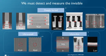
Explore how optical photonic metrology, broadband plasma, and actinic EUV drive sub-nm semiconductor yield, Market trends ($25B by 2031), and top vendors.
The exponential growth of AI training and inference clusters is reshaping global supply chains from silicon wafers to rare-earth magnets. This hub page aggregates factual insights, technical deep-dives, and structured summaries on the infrastructure, materials, and processes required to scale AI compute.
Explore how optical photonic metrology, broadband plasma, and actinic EUV drive sub-nm semiconductor yield, Market trends ($25B by 2031), and top vendors.
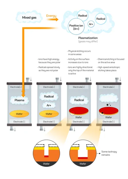
Explore how dry plasma and wet chemical etch machinery shape advanced semiconductor manufacturing, overcoming 2nm fabrication challenges and supply chain risks.
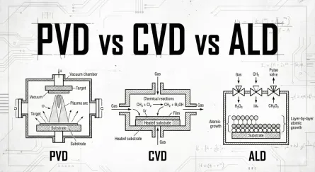
Discover how thin-film deposition (CVD, PVD, and ALD) powers AI hardware. Explore growth trends, top equipment suppliers, and sub-nanometer fabrication advances.
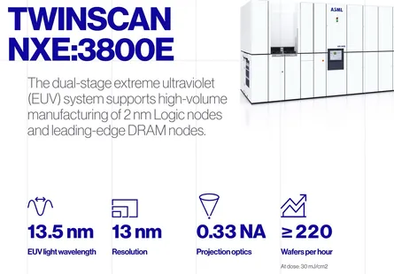
Discover the physics and engineering behind EUV lithography, from 13.5 nm laser-produced plasma and Zeiss optics to High-NA roadmaps and global supply chains.
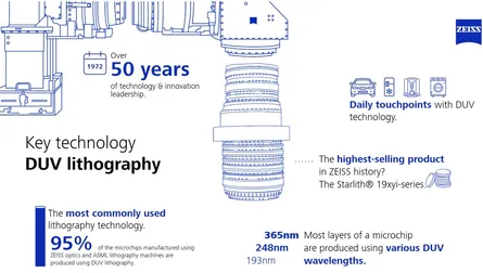
Discover why DUV lithography remains essential for semiconductor manufacturing. Learn how ASML immersion tools, multi-patterning, and hybrid scaling drive AI chip production.
Discover how Nanoimprint Lithography (NIL) enables low-cost, high-resolution photonics for AI data centers and silicon PICs. Explore Canon’s FPA-1200NZ2C, manufacturing challenges, market demand, and why NIL complements EUV in the AI semiconductor boom. Essential insights on process, firms, and future capacity.
Spruce Pine supplies 70–90% of global high-purity quartz (HPQ) for fused-quartz crucibles used in Czochralski growth of single-crystal silicon ingots at >1,425°C. Ultra-low metallic impurity levels (<50 ppb) are mandatory to prevent crystal defects that ruin yields in advanced sub-2nm AI accelerators.
ASML High-NA (0.55 NA) EUV systems shrink pitch to sub-10nm without multi-patterning. Pairing High-NA EUV with inorganic Metal Oxide Resists (MOR) offers higher etch selectivity and photon absorption, minimizing line-edge roughness for dense GPU transistor gates.
Gate-All-Around (GAA) nanosheets and 3D NAND (>300 layers) rely on dry plasma etching for high-aspect-ratio channel holes with sub-nanometer profile control. ALD then deposits uniform atomic-thin High-k dielectric films (Hafnium oxide) and contact metal liners (Tungsten) into 3D features.
At 800G and 1.6T transceiver speeds, copper interconnects suffer severe thermal dissipation and attenuation. InP-based laser modulators enable Co-Packaged Optics (CPO) and silicon photonics, cutting power per bit and latency across GPU cluster fabrics.
Transitioning server busbars from 48V to 800V DC reduces current by 16x, dramatically lowering copper resistive heat losses. High-coercivity Neodymium-Iron-Boron (NdFeB) magnets drive high-efficiency pumps and fans needed for direct-to-chip liquid cooling.
Indium, Gallium, and Germanium are byproduct minerals of zinc refining with inelastic supply. With China controlling 60–90%+ of refining and geopolitical concentration in noble gases (Neon, Krypton), supply chokepoints create persistent lead time risks for AI optics and chips.