SiC Power Wafers Powering AI Data Centers: Manufacturing, BPD Challenges & Gen 5 Breakthroughs
- David Rogers
- AI Buildout Supply Chain
- 2026-07-10
NEED TO KNOW
- Cutting AI Data Center Power Losses: Silicon Carbide (SiC) MOSFETs reduce power switching losses by >50% and support 800V DC architectures to solve GPU cluster power wall constraints.
- PVT Crystal Growth Challenges: Sublimating SiC powder at >2,000 °C via Physical Vapor Transport (PVT) is extremely slow (0.3–2 mm/h) and energy intensive.
- Basal-Plane Dislocation (BPD) Defect Limiter: BPDs represent the primary defect limiting yields and device reliability as the industry transitions from 150mm to 200mm wafers.
- Market & Supply Expansion: The SiC power device market is scaling to $11B by 2031, led by Wolfspeed (30–35% substrate share) alongside rapid expansion by STMicro, Infineon, and Chinese refiners.
Silicon carbide (SiC) power wafers are the critical enabler for the next wave of AI infrastructure. Hyperscale data centers running dense GPU clusters consume staggering amounts of electricity; traditional silicon power devices simply cannot deliver the efficiency, power density, and thermal performance required. SiC MOSFETs and diodes cut switching and conduction losses dramatically (often 50%+ vs. silicon), support higher bus voltages for slimmer distribution architectures, and reduce cooling overhead—directly addressing the power wall facing AI buildouts by hyperscalers /HIITIO/. The same technology is already transforming 800V electric vehicle drivetrains and renewable inverters, but AI data-center power supplies are now emerging as a powerful new growth vector /NVIDIA/.
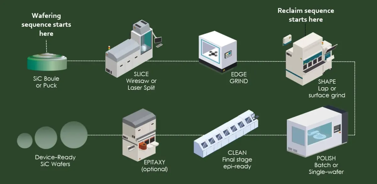
Manufacturing begins with ultra-high-purity SiC powder synthesized from abundant silica sand and carbon sources. The dominant industrial process is Physical Vapor Transport (PVT): the powder is loaded into a graphite crucible and sublimated at temperatures exceeding 2,000 °C under controlled vacuum and temperature gradients /ScienceDirect/. Vapor species (SiC₂, Si₂C, Si) transport and recrystallize onto a precisely oriented 4H-SiC seed crystal, slowly building a single-crystal boule at typical rates of 0.3–2 mm/h typically taking days to weeks. The boule is then ground cylindrical, sliced into wafers via multi-wire diamond sawing (managing kerf loss), lapped, ground, and finished with chemical-mechanical polishing (CMP) to achieve sub-nanometer roughness, extreme flatness, and minimal total thickness variation. Finally, high-temperature CVD epitaxy grows the thin, precisely doped device layers. Purity and crystallographic perfection are non-negotiable; even low densities of micropipes or dislocations destroy device yield and long-term reliability.
Key challenges include the inherently slow, energy-intensive growth and defect proliferation when scaling wafer diameters from today’s dominant 150 mm to 200 mm (and beyond). Among remaining defects, basal-plane dislocations (BPDs) have become the major limiter of long-term device performance and reliability /CS MANTECH/. Overall, larger wafers deliver roughly 30–33% more die per wafer, slashing cost per device once yields stabilize. Material and process advances are already delivering measurable gains, as demonstrated by Wolfspeed’s Gen 5 platform, whose 1200V MOSFETs achieve up to 27% lower specific on-resistance than current competitive solutions /Wolfspeed/. Innovations in thermal management during growth, advanced graphite furnace components, optimized slurries for faster/lower-damage polishing /ScienceDirect/, and emerging laser-based slicing or electrochemical mechanical polishing are all aimed at boosting throughput, cutting energy intensity, and improving yields.
Market momentum is exceptional. The global power SiC device market is forecast to reach approximately $11 billion by 2031, growing at a ~20% CAGR (2025–2031), propelled by EVs, renewables, and AI data-center power conversion /Yole/. Wolfspeed and others report strong sequential growth in the AI segment as hyperscalers redesign rack and facility power architectures around higher voltages and SiC efficiency. Wafer demand tracks this closely, with the substrate market itself expanding rapidly as device makers secure long-term supply.
Capacity is expanding aggressively while raw-material availability is not a constraint (silica and carbon are abundant; kerf-slurry recycling can recover SiC or produce silica). Wolfspeed remains the clear leader in high-quality substrates (roughly 30–35% share) with major U.S. investments including the Mohawk Valley 200 mm device fab and new crystal-growth facilities /Wolfspeed/. STMicroelectronics, Infineon, and onsemi pursue vertical integration strategies, while Chinese producers (TanKeBlue, SICC, etc.) are scaling rapidly to serve domestic EV and industrial demand /DigiTimes/. The current capacity build-out race also carries short-term oversupply risk, but the long-term trajectory driven by AI electrification and decarbonization points to sustained, strategically vital demand for secure, high-performance SiC wafer supply.
Key Insights
Why are silicon carbide (SiC) wafers crucial for AI data centers?
Silicon carbide (SiC) power wafers enable AI data centers to operate with far higher energy efficiency and power density. Unlike traditional silicon, SiC MOSFETs reduce switching losses by over 50%, support higher operating voltages (like 800V DC architectures), and tolerate higher temperatures. This directly tackles the power and cooling constraints faced by modern dense GPU clusters.
What is the primary defect challenge in physical vapor transport (PVT) growth of SiC?
Basal-plane dislocations (BPDs) are the most significant defect challenge in growing 4H-SiC crystals via the PVT method. BPDs can propagate into the epitaxial device layer, leading to electrical degradation and reduced reliability of high-voltage power devices. Reducing BPD density is a major focus for scaling from 150mm to 200mm wafers.
Who are the main Chinese suppliers of 6-inch and 8-inch SiC wafers?
The Chinese silicon carbide (SiC) wafer market is led by several key players in mainland China and Taiwan who are actively transitioning from 6-inch to 8-inch production. In mainland China, the market for 6-inch substrates has been dominated by companies like SICC (Shandong Tianyue), TankeBlue (Tianke Heda), Tongguang Crystal, Synlight Crystal (Shuoke), and San'an Optoelectronics. While all of these suppliers are upgrading to 8-inch capabilities, their commercial progress varies. Notably, SICC and TankeBlue achieved a historic breakthrough for the domestic industry by securing major wafer supply contracts with global semiconductor giants Bosch and Infineon, while San'an has partnered with STMicroelectronics to construct a joint-venture 8-inch SiC facility in Chongqing. Concurrently, Taiwanese suppliers—including GlobalWafers, Shengxin Materials (backed by Kenmec), Taiwan Applied Crystal (backed by Delta), Formosa Plastics Group, and Episil—are heavily targeting 8-inch wafers as their primary growth and cultivation sector.